Helical Logic
by
Ralph C. Merkle
Xerox PARC
3333 Coyote Hill Road
Palo Alto, CA 94304
merkle@xerox.com
www.ralphmerkle.com
and
K.
Eric Drexler
Institute for Molecular
Manufacturing
123 Fremont Avenue
Los Altos, CA 94022
http://www.foresight.org/FI/Drexler.html
This article has been published in
Nanotechnology (1996) 7 pages 325-339,
and is also available in HTML at:
http://www.zyvex.com/nanotech/helical/helical.html.
The HTML version differs in some respects from the published version.
Copyright 1992 by Xerox Corporation and the Institute for
Molecular Manufacturing.
All Rights Reserved.
Abstract
Helical logic is a theoretical proposal for a future
computing technology using the presence or absence of
individual electrons (or holes) to encode 1s and 0s. The
electrons are constrained to move along helical paths, driven
by a rotating electric field in which the entire circuit is
immersed. The electric field remains roughly orthogonal to
the major axis of the helix and confines each charge carrier
to a fraction of a turn of a single helical loop, moving it
like water in an Archimedean screw. Each loop could in
principle hold an independent carrier, permitting high
information density. One computationally universal logic
operation involves two helices, one of which splits into two
"descendant" helices. At the point of divergence,
differences in the electrostatic potential resulting from the
presence or absence of a carrier in the adjacent helix
controls the direction taken by a carrier in the splitting
helix. The reverse of this sequence can be used to merge two
initially distinct helical paths into a single outgoing
helical path without forcing a dissipative transition.
Because these operations are both logically and
thermodynamically
reversible, energy dissipation can be
reduced to extremely low levels. This is the first proposal
known to the authors that combines thermodynamic
reversibility with the use of single charge carriers. It is
important to note that this proposal permits a single
electron to switch another single electron, and does not
require that many electrons be used to switch one electron.
The energy dissipated per logic operation can likely be
reduced to less than 10-27 joules at a temperature of 1
Kelvin and a speed of 10 gigahertz, though further analysis
is required to confirm this. Irreversible operations, when
required, can be easily implemented and should have a
dissipation approaching the fundamental limit of ln 2 ×
kT.
Introduction
Trends in computer hardware are leading toward higher density
and lower energy dissipation. Ultimately, some approaches
should result in packing densities in excess of 1017 logic
devices in a cubic centimeter(Carter et al. 1988, Drexler
1992) (although the current proposal might require a somewhat
larger volume). The trend towards higher packing density
strongly influences energy dissipation. Conventional devices
must dissipate more than ln(2) × kT joules in switching; so
1017 conventional devices operating at room temperature
(ln(2) × kT ~ 3 ×
10-21 joules for T = 300 Kelvins) at a
frequency of 10 gigahertz would dissipate >3,000,000
watts; a computer with 1,000 times as many logic elements
would still be of reasonable size but would dissipate
3,000,000,000 watts.
Conventional devices actually perform more poorly. Even an idealized
device which used a one volt power supply and dissipatively
discharged a single electron to ground during a switching
operation would dissipate one electron volt per switching
operation. At T=300 Kelvins, this is 40 × kT per switching
operation or about 160,000,000 watts for a computer with 1017
logic elements operating at 10 gigahertz. If each switching
operation involves hundreds of electrons then energy
dissipation enters the multigigawatt range.
New thermodynamically reversible circuits (including CMOS,
nMOS and CCD-based logic circuits(Hall 1992, Merkle 1993c,
Younis and Knight 1993, Koller and Athas 1992, Merkle 1992))
would fare better, but these circuits still have dissipative
losses caused by the resistance of the circuit. While
resistance in sufficiently small wires can be very low(Sakaki
1980), if such wires are connected to each other, to logic
elements or to larger structures it is common to find
resistances of the order of 13K (half of h / e2, where h is
Planck's constant) (note that no claim is made that the
successful operation of such circuits must fundamentally
require resistances of this magnitude, we simply note that
shrinking current circuits to a small scale would result in
such resistances: further research in this area might be
successful in dealing with this problem). Assuming that 100
electrons were required to charge and discharge the wires and
capacitive loads in each logic element, and assuming a
resistance of approximately 13K, we would still find our
1017 gate computer dissipating tens of megawatts even using
these particular thermodynamically reversible methods.
(half of h / e2, where h is
Planck's constant) (note that no claim is made that the
successful operation of such circuits must fundamentally
require resistances of this magnitude, we simply note that
shrinking current circuits to a small scale would result in
such resistances: further research in this area might be
successful in dealing with this problem). Assuming that 100
electrons were required to charge and discharge the wires and
capacitive loads in each logic element, and assuming a
resistance of approximately 13K, we would still find our
1017 gate computer dissipating tens of megawatts even using
these particular thermodynamically reversible methods.
If the exponential trends of recent decades continue, energy
dissipation per logic operation will reach kT (for T=300
Kelvins) early in the next century(Landauer 1988). Either
energy dissipation per logic operation will be reduced
significantly below 3 × 10-21 joules, or we will fail to
achieve computers that simultaneously combine high packing
densities with gigahertz or higher speeds of operation.
There are only two ways that energy dissipation can be
reduced below 3 × 10-21 joules: by operating at temperatures
below room temperature (thus reducing kT), or by using
thermodynamically reversible logic. Low temperature
operation doesn't actually reduce total energy dissipation,
it just shifts it from computation to refrigeration (Halliday
and Resnick 1988). Thermodynamically reversible logic
elements, in contrast, can reduce total energy dissipation
per logic operation to << kT. This paper analyzes a
proposed thermodynamically reversible single electron logic
system. To achieve high reliability while switching single
electrons, we analyze operation at ~1 Kelvin.
Reversible Architectures and Logic Proposals
One concern about this approach is the need to use reversible
computer architectures. Such architectures are entirely
feasible(Landauer 1988, Fredkin and Toffoli 1982, Bennett
1982, Bennett 1988, Bennett 1989, Merkle 1993b, Ressler 1981,
Hall 1992, Fredkin and Toffoli 1978, Seitz et al. 1985,
Merkle 1993c, Landauer 1961, Landauer 1981, Bennett 1973,
Younis and Knight 1993) and will not be discussed further
here. Bennett(Bennett 1989) has proposed very general
methods for converting arbitrary irreversible computations
into time and space efficient reversible computations.
A wide variety of reversible device proposals have been
made(Drexler 1988, Likharev 1982, Likharev et al. 1985,
Drexler 1992, Fredkin and Toffoli 1978, Seitz et al. 1985,
Merkle 1993c, Younis and Knight 1993, Koller and Athas 1992,
Merkle 1992). The present proposal is abstractly similar to
billiard ball logic(Bennett 1985, Fredkin and Toffoli 1982),
and in particular uses the concept of a "switch gate" or
"interaction gate."
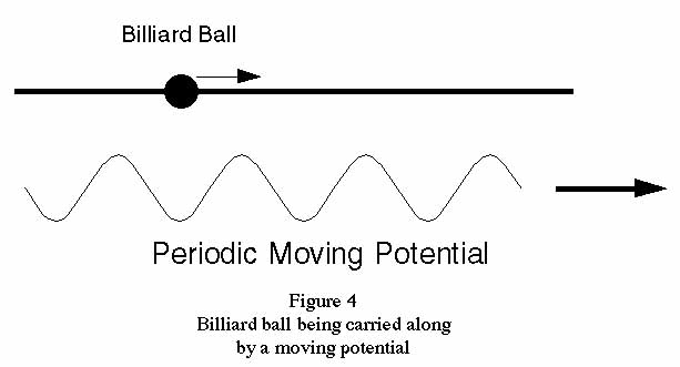
In billiard ball logic(Fredkin and Toffoli 1982), a set of
billiard balls are fired into a set of immovable reflectors
at a fixed speed. As the billiard balls bounce off each
other and off the reflectors, they perform a reversible
computation. Provided that the collisions between the
billiard balls and between the billiard balls and the
reflectors are perfectly elastic, the computation can proceed
at a fixed finite speed with no energy loss.
As originally proposed, this "ballistic" model of
computation suffers from the shortcoming that the positions
of the reflectors and the initial velocity of the billiard
balls must be perfectly accurate. In the real world, the
computation would rapidly deteriorate into chaos unless some
restoring force maintained the alignment of the billiard
balls. Landauer(Landauer 1981) proposed exactly this,
suggesting that the billiard balls should remain in the
trough of a moving periodic potential (illustrated in Figure
4).
Billiard ball logic is usually thought of in connection with
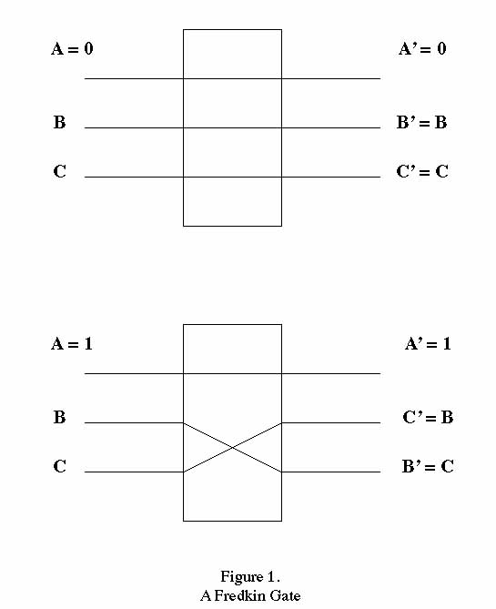
Fredkin gates(Fredkin and Toffoli 1982). Fredkin gates are
conservative three-input three-output gates that are
logically complete, i.e., any computation can be implemented
by an appropriately connected set of Fredkin gates. An
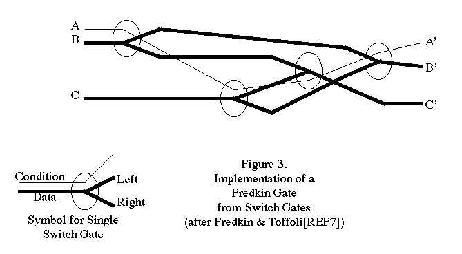
appropriately arranged set of reflectors can be used to
implement a Fredkin gate from billiard balls. Rather than
considering the Fredkin gate we will focus instead on the
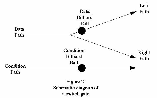
switch gate(Fredkin and Toffoli 1982). This can be used to
make a Fredkin gate (and so is also logically universal) but
it is physically simpler and easier to implement.
A Fredkin gate is illustrated in Figure 1, a switch gate is
illustrated in Figure 2, a method of implementing a Fredkin
gate from switch gates is shown in figure 3, while a billiard
ball being carried along by a periodic potential is shown in
Figure 4.
While the abstract concept of billiard ball logic has been
known for some time, the idea of implmenting this approach by
replacing the billiard balls with charged particles is
surprisingly recent(Merkle 1993c) (though Landauer(Landauer
1981) did refer to an unspecified short range repulsion). In
the present proposal, we replace the billiard ball with a
single electron. While other charged particles or charged
packets of particles can be used, we will focus on the single
electron implementation because of the obvious long term
performance advantages. The concept that future electronic
devices might use single electrons is becoming more
accepted(Likharev and Claeson 1992, Washburn 1992, Grabert
and Devoret 1992). This is the first description of a
thermodynamically reversible switching device using single
electrons. Not only are we switching single electrons, we
are also using single electrons to control the switching
(unlike many proposals which require many electrons to switch
a single electron). It is plausible that thermodynamically
reversible single electron switching devices will be the
ultimate evolutionary end point of electronic logic devices.
The authors emphasize that other proposals for single
electron thermodynamically reversible logic devices will
certainly be advanced, so the present proposal must be viewed
as the first in a class rather than "the" one and only
design for a single electron thermodynamically reversible
logic device.
While the analysis here focuses on the case of a "charge
packet" consisting of a single electron, the use of a multi-
electron charge packet would clearly be simpler in terms of a
more near term implementation. In particular, charge packets
are commonly used in CCD's. By making a series of design
choices in favor of near term feasibility we can arrive at a
design which is basically a thermodynamically reversible type
of CCD logic. This possibility is discussed more fully in
(Merkle 1993c). The performance of such a system would
likely fall well short of ultimate limits for pragmatic
reasons. The present paper focuses on an approach which
should be feasible in the long term (though less likely to be
practical in the near term) and which offers the possibility
of greatly superior performance and, in particular, the
possibility of very low energy dissipation while still
operating in the gigahertz range or higher.
Clock Distribution using Rotating Electric Fields
The periodic moving potential (illustrated in figure 4) which
drives the electrons forwards can be viewed as a periodic
clock signal. It is conventional in today's circuits to
distribute clock signals using wires. This approach is
energetically disadvantageous because the propogation of the
clock signal through wires is itself dissipative, as well as
requiring a complex (and space consuming) network for
distribution. An attractive alternative is to use time
varying electric fields. We propose the use of rotating
electric fields as these are conceptually simple, easy to
produce, and adequate to drive a wide range of logic
devices.
The picture of clock distribution being proposed here is new
(though it is abstractly similar to the rotating magnetic
field used to clock and power magnetic bubble devices(Bobeck
and Scovil 1971, Kinoshita et al. 1976)). The computing
element is immersed in a rotating electric field. The
electric field, and hence the clock, is available at every
point in the device and yet no wires are required to
distribute it. This reduces energy dissipation and
eliminates the space that would otherwise be occupied by the
clock distribution network.
A rotating electric field is rather different from a periodic
moving potential. In order to achieve the same effect (i.e.,
to move electrons forwards along their path) we propose the
use of helical paths, with the electric field rotating at
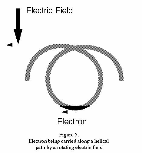
right angles to the axis of the path. The electron will be
confined to part of a single turn of the helix and as the
electric field rotates the electron will be moved along the
helical path much as water is moved along an Archimedes
screw. This is illustrated in figure 5.
If we were to examine the potential at any point along the
helical path we would find that it varied in a sinusoidal
fashion much as the potential varies along a straight path
under the influence of a moving periodic potential. The use
of a periodic moving potential with straight paths (as shown
in figure 4) and the use of a simple rotating electric field
with helical paths produce very similar results. In either
case, the electron is moved along the path.
There are other methods of providing a moving periodic
potential that do not involve distribution of clock signals
through wires. A simple proposal would be to have a circuit
on the surface of a rotating disk, with an opposing disk with
fixed charges on it. The relative motion of the two disks
would result in a moving potential that would clock the
circuit. Alternatively, instead of disks two tubes of
differing diameter, one tube placed inside the other, could
be used. Circuitry could be placed on the inner surface of
the outer tube, while fixed charges could be placed on the
outer surface of the inner tube. Again, relative motion of
the inner tube with respect to the outer tube could provide a
moving potential. This approach also has the advantage that
the tubes could be reduced in radius to a very small size
(nanometers) and the rotational speed of the inner tube could
be made very high (gigahertz) without any fundamental
problems. Many such tubes could be stacked adjacent to each
other, and charged particles being swept along a potential on
one tube could move to an adjacent tube, provided that the
movements of the clocking potentials in the two adjacent
tubes were appropriately synchronized. A different approach
would be to operate the circuit on a piezomechanical surface
in which surface acoustic waves created a moving electric
potential.
We will not consider the many possible alternatives in this
paper.
The Basic Idea
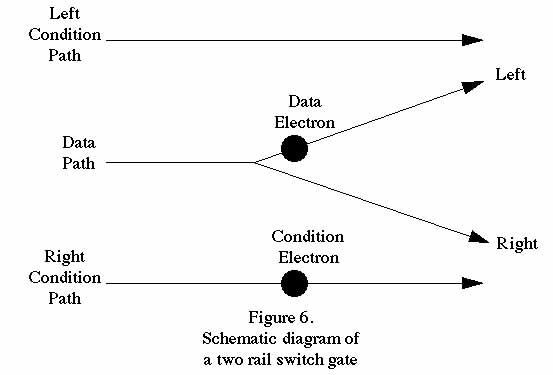
In helical logic, information is encoded in the presence or
absence of individual electrons. Electrons are moved from
place to place along helical paths. When two helical paths
are brought into close proximity the electrons interact
through electrostatic repulsion, thus producing an electronic
switch gate. The electronic switch gate involves two
incoming and three outgoing helical paths. One incoming
helical path is termed the "data" path while the other is
termed the "condition" path. The two descendants of the
data path are called simply the "left" and "right" paths.
The electron in the data path will be steered to either the
left or right path depending on the presence or absence of an
electron in the condition path. This is illustrated
schematically in figure 2, but with the billiard balls replaced
by electrons.
The reverse of this operation, in which three incoming
helical paths produce two outgoing helical paths, is similar
but "run backwards" in time. Because the basic operation
of a switch gate is reversible, it can be operated in either
the forwards or reverse direction. We will therefore not
explicitly analyze this process. Note that in reverse
operation it is essential that the presence or absence of a
charge carrier on the data path be correctly correlated with
the path (left or right) along which the switched charge is
entering the switch gate. This constraint can be met (as
illustrated in figure 3 showing the design of the Fredkin
gate).
It is worth noting that irreversible operations are sometimes
convenient. A basic irreversible operation in helical logic
merges two incoming helical paths into one outgoing helical
path (and dispenses with the data path). Such an
irreversible logic operation, if properly designed, should
have an energy dissipation which approaches the fundamental
limit: ln 2 kT. Helical logic has the valuable ability to
degrade gracefully when irreversible operations are
required.
We will focus primarily on fundamental issues of device
performance while neglecting the issues involved in
manufacturing any specific device. Thus, we will simply
assume that the ability to economically manufacture
atomically precise semiconductor material, with dopant atoms
placed at atomically precise lattice coordinates, is
available. Such a manufacturing technology is not available
today but should be available at some point in the
future(Drexler 1992, Merkle 1994). In the long run, if we
are to achieve the maximum performance possible from
semiconductor devices, we will have to develop and use some
sort of molecular manufacturing technology. This is true
almost regardless of the specific details of the device
proposal. The more precisely a device can be fabricated,
the better the achievable performance. The limit of this
trend will be devices in which each atom is in the right
place.
There are many choices for the materials that comprise the
helical path and the surrounding medium. An obvious choice
is GaAs and AlAs(Sze 1990). Electrons prefer GaAs to AlAs by
about 0.3 ev(Van de Walle 1989), so by operating at a
sufficiently low temperature complete confinement of the
electrons could be achieved. Another choice would be Ge and
Si(Sze 1990, Bean 1992). Other possibilities that should
become feasible in the future with the advent of molecular
manufacturing(Drexler 1992, Feynman 1960), would be Si and
GaP(Sze 1990), Si and ZnS(Sze 1990), or even C (in the form
of diamond) and vacuum. The latter would offer significant
advantages because of the low dielectric constant of vaccuum,
although the negative electron affinity of the hydrogenated
diamond (111) surface suggests that either the use of holes
as the charge carriers or the modification of the diamond
surface to achieve a positive electron affinity (i.e.,
fluorinated diamond (111)) would be advantageous. If the
helical channels are diamond with hydrogenated diamond (111)
surfaces, an electron in the channel would tend to escape
into the surrounding vacuum. The idea that a hole might
perform a similiar feat is less plausible. Diamond channels
with fluorinated surfaces in vaccuum using either electrons
or holes (or both) as charge carriers might be an attractive
choice once our manufacturing technology is able to build the
required structures.
The negative electron affinity of the hydrogenated (111)
diamond surface also suggests the use of an evacuated channel
surrounded by walls of diamond. This approach means the
channels are holes bored in a block of diamond. The motion
of electrons through evacuated channels might prove
advantageous by reducing electron/channel interactions. The
creation of a helical tube with relatively smooth walls in a
block of unstrained diamond would require the use of more
than just the (111) plane. Other surfaces (e.g., (100) or
(110)) could be used and would permit a tube with smoother
walls. Approaches using strained diamond (e.g., diamond
which is curved by, for example, the introduction of
appropriately placed dislocations (Merkle 1993a)) would be
another alternative.
The use of other charge carriers produces a wider range of
possibilities. For example, the charge carrier could in
principle be a single proton. The channels would then be
pores through which H+ could easily move. The increased mass
of H+ (as compared with an electron) would simplify
confinement by decreasing the effective distance through
which the charge carrier could tunnel. Channel size and
interchannel distances could both be made much smaller;
proton-proton repulsive interactions would therefore be
larger and operating temperature could be increased. The
smaller size and higher operating temperature of a helical
logic system based on hydrogen ions would compensate to some
extent for the slower speed, and the result might be
advantageous in some applications. Many other small ions
could also be used.
The use of charge packets made up of many electrons (or
holes) should provide a method of implementing helical logic
using today's technology at higher temperatures. The use of
charge packets is common in CCDs. It is an open question
whether today's technology can economically mass produce the
complex structures needed for helical logic (though research
devices should be feasible). However, a 2D version of
helical logic which used spiral paths should be feasible with
today's technology. The implementation of a planar switch
gate should likewise be feasible. More research on this
point would be worthwhile.
Whatever the materials choice and manufacturing technology,
the primary requirement is that a charge carrier be confined
to a helical path, and be able to interact with other charge
carriers in other helical paths.
Energy Dissipation
Energy dissipation is caused by three main factors: energy
loss during charge transport, energy lost to the material in
the absence of charge carriers (the dielectric loss factor),
and energy loss during switching operations. All three loss
mechanisms are a function of clock frequency. We will call
these transport loss, dielectric loss
and switching loss.
Energy loss will also occur when irreversible logic
operations occur. We will neglect this source of energy loss
in the following analysis, as it will vary widely depending
on the logical design of the system and possibly the specific
algorithm being used.
Transport losses
While electrons moving in bulk material are subject to
scattering and resistive losses, an electron confined to a
portion of a helix at a sufficiently low temperature is
almost always in its ground state. The interactions between
the electron and the lattice should be greatly diminished,
particularly if the energy of the ground state is several
times kT below the energy of the first excited state.
Conventional resistive losses should be very greatly
reduced.
It is important to distinguish between charge transport in
helical logic and charge transport along a wire, even a very
fine wire. The mobility of an electron confined to a
one-dimensional wire can be much higher than in the bulk
material(Sakaki 1980). However, even in this case the
electron is confined in only two dimensions and can move
freely along the third. In helical logic, by contrast, the
electron is confined in all three dimensions. Viewed from
the frame of reference of the moving electron, it is simply
sitting at the bottom of a potential well.
Lattice vibrations induced by the moving charge will cause
transport losses. Treating the electron as an isolated
charge subject to an oscillating force F, we have(Drexler
1992, page 164):
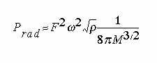
Prad is the radiated power, F is the force applied to the charge,
 is the frequency in radians per second,
  is the density, and M is a modulus of elasticity.
For an electric field E of 108 volts/meter (106 volts/centimeter,
well below the breakdown strength of diamond) we have a force F on a single
electron of 1.6 × 10-19 × 108 = 1.6 × 10⁻¹¹
N. The density of diamond is about 3,500
kg/m3. The frequency in radians
per second for a 100 picosecond time to make a single rotation is 2  × 1010. M is about 1012 Pascals. Substituting these
values into equation (1) yields a radiated power of roughly 2.4 × 10⁻¹⁸
watts, or 2.4 × 10⁻²⁸ joules per charge carrier per rotation
of the electric field.
× 1010. M is about 1012 Pascals. Substituting these
values into equation (1) yields a radiated power of roughly 2.4 × 10⁻¹⁸
watts, or 2.4 × 10⁻²⁸ joules per charge carrier per rotation
of the electric field.
This treats the electron as an isolated point charge, and
also uses an approximation which should be accurate at
frequencies well below the Debye frequency. The frequency
selected is below the Debye frequency for diamond, while the
error caused by the point charge assumption is conservative
(in the sense that this assumption makes the energy
dissipation higher than one would otherwise expect).
Lower power dissipation should be feasible. We could
maintain approximate charge neutrality by placing a fixed
charge in the neighborhood of the electron. A donor atom
contributing a positive charge will effectively cancel the
negative charge of the electron. This is likely to produce a
lower energy dissipation, as acoustic energy radiated from a
dipole is lower than that radiated from a monopole (when the
wavelength of the radiation is longer than the distance
between the charges in the dipole). Alternatively, we could
represent a logic "1" by the presence of an electron and a
hole. The resulting dipole could then be transported along
two helices ("double helix logic") or both the electron and
the hole could be confined in a single helix, one of them
being half a turn ahead of the other. In the latter case,
two types of dipole would be possible: one in which the
electron precedes the hole, and another in which the hole
precedes the electron. While it might appear paradoxical to
have a helix which can simultanesouly confine both an
electron and a hole, diamond helices with fluorinated
surfaces in vacuum should (as noted earlier) be able to do
exactly that.
A frequency of 1010 hertz, along with the assumption that a
single turn of the helix has a diameter of about 100
nanometers, implies that the electron is moving at a speed of
about 3-4,000 meters per second (below the speed of sound in
diamond). The dissipation mechanisms that might come into
play for significantly higher speeds are not analyzed
here.
Accelerations caused by variations in the helical structure
for the purpose of altering the direction of charge transport
will result in accelerations of the charged particle that
might well result in radiative losses. Radiative losses are
discussed further under switching losses, as accelerations of
the charged particles during switching can likewise result in
radiative losses.
Dielectric Loss
The dielectric loss can be quite small. The highest
experimental quality factor (Q ) for a superconducting cavity
resonator with a vacuum interior was 5 × 10¹¹ at a frequency
of 10.5 GHz and a temperature of 1.3 K. Experimental values
for Q for cavity resonators at low temperatures (a few
Kelvins) with saphire interiors are above 108 at a frequency
of a few gigahertz, while Q's of 1015 are in principle
feasible for defect-free saphire at 2 Kelvins and about 3
gigahertz(Braginsky 1985). For defect-free materials well
below the Debye temperature, Q can increase as 1/T5
or 1/T4
as the temperature T is decreased(Braginsky 1987, Gurevich
1979, Gurevich and Tagantsev 1991). It is reasonable to
expect that the Q for defect-free diamond (a semiconductor
which could be used for electronic devices) would be better
than that for saphire. These results are for a solid block
of homogeneous material, while an actual computer would have
irregularities and inhomogenieties associated with the charge
transport and switching devices, as well as the mobile charge
carriers needed to propagate information. As a consequence,
the Q for a computing device is likely to be different than
the Q for a homogeneous material. Some analysis of this is
done below, but this area requires further investigation
before definitive statements about the dielectric loss for a
real system can be made.
Dielectric losses for bulk silicon and diamond are described
in (Braginsky 1985, Braginsky 1987, Gurevich 1979, Gurevich
and Tagantsev 1991) by the equation:
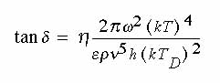
Where  is a dimensionless anharmonicity
parameter with typical values between 10 and 100,
is the frequency in radians per second, e is the dielectric permittivity
of the crystal, the density, h is
Planck's constant, v the speed of sound, k is Boltzmann's constant,
T the temperature in Kelvins, and TD the Debye temperature.
Note that Q ~ 1/(tan
is a dimensionless anharmonicity
parameter with typical values between 10 and 100,
is the frequency in radians per second, e is the dielectric permittivity
of the crystal, the density, h is
Planck's constant, v the speed of sound, k is Boltzmann's constant,
T the temperature in Kelvins, and TD the Debye temperature.
Note that Q ~ 1/(tan  ).
).
In the case of diamond and approximating the value of
as 100(Braginsky 1987) we can approximate the loss factor.
If we use
= 2 × 10¹⁰, k = 1.38
× 10-23, T = 1 K, e = 5.7,
= 3,510 kg/m3, h = 6 × 10-34, TD
= 2340, v ~ 15,000 m/s; then we get tan
~ 10-20. (Experimental tan 's for
saphire of less than 10-9 at a frequency of about 10 gigahertz at
a temperature of 1.5 Kelvins have been observed(Braginsky 1987). Saphire has
a fundamentally higher tan because of its
crystal symmetry). If we assume (rather generously) that each switch is a cube
100 nanometers on a side, and if we further assume that ten times this volume
might be required for interconnections between switches (again rather generous),
we have a total volume per switch of 107 cubic nanometers. The energy
stored by an electricic field of 108 volts/meter in this volume results
in an energy of about 2.5 × 10⁻¹⁵ joules per gate (assuming
a dielectric of 5.7, as before). Multiplied by our dielectric loss factor, we
get an energy loss of under 10-34 joules per cycle per gate.
The form of the equation governing the dielectric loss varies
greatly depending on the crystal symmetry. For example,
centrosymmetric crystals of the D6h symmetry group have a
dielectric loss that falls off as T9 (linear falloff in
frequency, but ninth power in the temperature), while
dielectric loss for crystals of the Ci
symmetry group falls
off as 5T(Gurevich and Tagantsev 1991).
The presence of the helical paths creates a non-uniform
structure, and hence induces additional losses. A loss
mechanism suggested by Soreff(Soreff 1994) is caused by
forces acting between induced dipoles. Even when charge
carriers are completely absent the rotating electric field
will induce dipoles in the helical paths because the
dielectric constant of the path and of the surrounding medium
typically differ. A single half-turn of a helical path of
the dimensions considered here can be approximated as a
column about 100 nm long by 10 nm deep and 10 nm wide. If
the electric field is 108 v/m and we assume the disparity of
the dielectric constants of the path and of the medium is
approximately 5.7 (as would be the case for diamond helical
paths), such a volume would have an induced dipole moment of
roughly 5 × 10-26 C-m. Two such dipoles at a distance of
roughly 100 nm (i.e., the opposing halves of a single helical
turn) will experience a repulsive force of under 10-12 N
(using a formula derived from that for the interaction energy
given in (Israelachvili 1992)). Recall that the helical
track is already being subjected to forces caused by the
charge carrier, estimated above as 1.6 × 10⁻¹¹ N, and that
the energy dissipation is a function of the square of the
force. Thus, the inter-track repulsive forces caused by
induced dipoles are in this approximation smaller than the
forces caused by a charge carrier by at least an order of
magnitude. Because the inter-track spacing is small compared
with the acoustic wavelength, dissipation from this mechanism
should be further substantially reduced.
The actual dielectric losses in a complex three dimensional
structure consisting of numerous very small logic gates are
certain to be different from the value estimated here for a
perfect diamond crystal. However, it seems unlikely that
such losses must necessarily be much larger and they can
likely be made much smaller. The wide variation of
dielectric loss among crystal types suggests that careful
selection and design of materials can be used to make systems
with very low dielectric losses. The uncertainty in the
dielectric loss remains substantial, however, and the actual
loss could potentially be significantly higher than estimated
here.
Switching Losses
Switching times need not be the same as the reciprocal of the
clocking frequency. A single switching event could take
place as the charges moved a fraction of a single helical
turn, or could be spread out over many helical turns.
The reader who wants to think about a single specific
geometry while reading the analysis in this section can read
the geometry of a specific switch gate in the first three
paragraphs of the section titled "Quantum Mechanical
Analysis of the Operation of a Specific Switch Gate."
Switching losses occur because the two electrons are excited
by their interaction and will dissipate energy when they fall
back to their ground state. If we can keep the two electrons
from entering an excited state, we can avoid energy
dissipation.
A rather interesting observation is that switching losses
caused by this mechanism can in principle be avoided almost
completely even if the two electrons do enter excited states.
An electron is in an "excited" state only with respect to
some potential energy function. For any given wave function,
however, there exists a potential energy function for which
that wave function is the ground state. Thus, if we knew the
wave function of each electron as it left the switch gate,
and if we could engineer the path along which the electron
moves to have the appropriate potential energy function, then
the energy dissipated by the electron could in principle be
eliminated.
Put more generally, if we know the state of a system then we
need not (in principle) dissipate any energy at all.
Unfortunately, it would seem that the wave function of an
electron leaving a switch gate depends on the presence or
absence of the other electron. Even if both electrons
entered the switch gate in their ground state, and even
though the evolution of the wave function is deterministic,
if we look only at one of the departing electrons we will
find it in one of two states depending on the presence or
absence of the other electron.
This can, in general, be solved by the use of the
"interaction gate"(Fredkin and Toffoli 1982) illustrated in
figure 7.

In the interaction gate two electrons enter along two paths
(A and B), and depart by four paths. Again, the interaction
gate can be used to implement a Fredkin gate, and so it is
logically complete. What makes the interaction gate
interesting is the following property: if we know that an
electron is present on a particular output path, then we know
the inputs to the gate. For example, if an electron leaves
the interaction gate along the A left path, then we know that
there was an electron on path B (or else the electron would
have left the gate on the A right path). Thus, we can
engineer the precise geometry and potential of the A left
path knowing exactly what state the electron is in when it
travels along that path.
Similar observations hold for all other ways in which an
electron can leave the interaction gate, and so by
appropriate engineering of the outgoing paths we can
essentially eliminate energy dissipation from this source.
When a charge is switched down one of two alternate paths (as
happens to the data electron in figure 6) it is subjected to
an arguably unpredictable acceleration (we don't know which
path it's going to take) which will in turn generate an
arguably unpredictable pattern of radiation. If we assume
that the accelerations involved are similar to those that
would occur in an oscillating dipole, we can readily estimate
the magnitude of this loss by using the formula for the power
radiated by an oscillating point charge(Feynman 1963), page
32-3]:
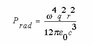
Dividing the radiated power by the frequency gives the energy
dissipated per cycle, which is:
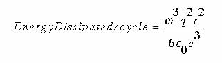
For f = 10 gigahertz and r = 50 nanometers (and neglecting
the dielectric constant of the medium) this results in losses
of about 10-35 joules per cycle.
Although this is a reasonable approximation to the energy
losses caused by the acceleration of a single charge during
the switching process, as noted earlier the switching
frequency and the frequency of the externally applied
electric field need not be exactly the same. Likewise, the
distance which the switched and switching charges must
traverse during a switching operation is different from the
radius of the helix, and the acceleration profiles need not
be sinusoidal. Further, modifications to the helical
structure to transport charge carriers to various more or
less random locations required by the computation will result
in accelerations unrelated to switching.
Despite these admittedly rough approximations, the low
dissipation computed suggests that this mechanism will not be
the dominate source of energy dissipation under the
conditions considered in this paper.
Because the energy dissipated per cycle is a function of the
square of the charge, and because it might happen that many
switches simultaneously switch charge in the same direction
(thus effectively increasing the charge that is being
accelerated) the energy dissipation from this mechanism might
be increased significantly. This could be reduced by careful
design of the switching operations to reduce the likelihood
of such an event. Even stronger, if double helical logic is
employed then a single switching operation could be so
designed that it simultaneously accelerated both an electron
and a hole in the same direction and by the same amount.
This should effectively reduce energy dissipation from this
mechanism by many orders of magnitude.
We assume that acoustic losses caused by the switching
operation are similar to or smaller in magnitude than the
acoustic losses caused by charge transport.
Quantum Mechanical Analysis of the Operation of a
Specific Switch Gate
General
This analysis considers the behavior of a two-rail
single-electron switch gate (figure 6, below). Note that the "two-rail"
switch gate is similar to but distinctly different from the
single-rail switch gate discussed earlier. In the two-rail
variant, the single condition path is divided into two
condition paths: a left condition path and a right condition
path. There will always be one switching electron, entering
either from the left or the right condition path. The
switching electron is assumed to be in a narrow potential
well that effectively confines it to a small region, assumed
to be a point charge. The switched electron, by contrast, is
assumed to be in a relatively wide harmonic potential, and it
will be necessary to compute the wave function of the
switched electron in this potential during the switching
process. Although the switch gate is really a three
dimensional structure, we will "unroll" the coordinate
systems for this analysis. The z axis will measure
"distance along the helix." The wave function of the
switched electron is assumed to be confined to an x-y plane
at any given moment in time, although the z coordinate of the
plane will move forwards as the switching process unfolds.
The y coordinate for each path does not vary with time. The
condition path is assumed to be a few nanometers "above"
(located closer to the principal axis of the helix) the data
path, i.e., the y coordinates of the data path and the
condition path differ by a few nanometers. This implies that
the x coordinates of the condition and data paths can vary
independently with no risk that the two paths will collide
and merge their contents.
This geometry can be visualized in the following way: think
of the condition paths as being wrapped helically around one
tube, and the data paths as being wrapped helically around a
second tube of slightly larger diameter. Now, insert the
smaller tube into the larger tube and align the switching
region of the data paths with the appropriate region of the
condition paths. As the diameters of the two tubes are
different, the electrons moving along a helical path on one
tube can't move onto a helical path along the other tube.
Only their electric fields will interact, allowing an
electron on one tube to "push" the electron on the other
tube down one of two alternative pathways.
Another way of thinking of the geometry of this switch gate
starts by considering the diagram of figure 6. Move the two
condition paths above the plane of the paper (move the two
condition paths towards you as you look at figure 6 -- this
movement is orthogonal to the plane of the paper) by some
short distance. This effectively moves the condition paths
out of the plane of the data paths, and allows the condition
and data paths to move up and down freely without any risk
that they will collide and merge their contents. Note that
"up" and "down" in this context are defined relative to
figure 6 -- the switched data electron moving along the left
path is moving "up". Finally, wrap figure 6 into a helical
tube by raising the upper left and lower right corners
towards each other.
The analysis that follows shows that a "plausible"
potential exists which simultaneously provides a low energy
dissipation and a low error rate at a reasonable switching
speed. The underlying heuristic guiding its design was to
minimize excitation of the switched electron during the
switching process. The switched electron is assumed to have
a significant probability of being excited, a probability
which must be analyzed and minimized. Such excitation leads
to both energy dissipation and to errors. By minimizing the
excitation, both problems can be reduced.
The authors expect that significantly better potentials are
feasible.
Standard SI units are used throughout.
Slow switching
Slow switching processes in single-charge helical logic
systems are straightforward: the underlying potential along
the paths through the gate (determined by the structure of
the device) evolves from one well to two, while the proximity
of the switching charge raises the potential energy in the
blocked path relative to that of the open path so that the
ground state of the switched charge remains bound in the
deeper well on the open path. In the limit of slow motion and
low temperature, the probability of the charge remaining in
the ground state can be made arbitrarily close to one, hence
the probability of an error (which requires a higher energy
state) can be made arbitrarily small. As will be seen, the
energy difference between the ground state and the excited
states that can evolve into states occupying the blocked well
can be made to exceed  E
= 10-21 J, hence the
probability that the blocked well will be occupied via
thermal excitation (on the order of exp(-E/kT)) is less than
10-30 for temperatures of ~1 K. Accordingly,
thermally induced errors can be made negligible. The chief
source of errors in faster switching processes will be
excitation resulting from nonadiabatic evolution of the
system.
E
= 10-21 J, hence the
probability that the blocked well will be occupied via
thermal excitation (on the order of exp(-E/kT)) is less than
10-30 for temperatures of ~1 K. Accordingly,
thermally induced errors can be made negligible. The chief
source of errors in faster switching processes will be
excitation resulting from nonadiabatic evolution of the
system.
The switching time proposed is a few orders of magnitude
slower than the period of a single oscillation of the
switched electron when excited to the first excited state.
This speed allows us to use the adiabatic approximation in
computing the wave function of the switched electron, in
estimating the probability of error, and in estimating the
energy dissipation. Faster switching times should be
feasible but would require a more detailed (and complex)
analysis.
Tailoring the potential function
Minimizing the error rate at a given switching speed requires
accurate control of the underlying potential, achieved by
some combination of bandgap engineering, modulation of well
geometry, and manipulation of the local electrostatic
environment (the distribution of charges, dipoles, and local
dielectric constants). The following analysis assumes that
the potential can be modulated by a tenth of an eV or more in
essentially any smooth pattern. Analysis of a related problem
(barrier heights of two surfaces sliding against each other)
using a simple Monte Carlo technique makes this assumption
plausible(Drexler 1992, page 278). For mathematical
convenience, this analysis examines a potential with
discontinuous first derivatives; smoother potentials (e.g.,
the present potential convolved with a suitable Gaussian) can
have superior properties.
Variations in potential along the z axis are limited in
frequency by the spacing of the atoms, and are further
effectively limited by the fact the wave function will have
some spread along the z axis. As a consequence, we have
limited ourselves to a potential that varies relatively
slowly with changes in the z coordinate. Variations in
potential along the x axis involve tens of nanometers, and so
could reasonably be engineered by appropriate placement of
individual atoms. The potential along the y axis is assumed
to confine the electron to a fixed distance from the axis of
the helix, i.e., the electron is confined to a helical
ribbon.
Non-thermal excitation and nearly-harmonic
potentials
Each charge is assumed to be in its ground state as it enters
the switch. An error is assumed to occur when a charge is
excited to an energy level high enough to permit it to occupy
a secondary potential well on the blocked path. (This is a
conservative criterion: not all charges with sufficient
energy will in fact exit along the blocked path.) For error
rates to be low excitation probabilities must be small and
the evolution of the system must be nearly adiabatic. An
expression for the total probability of a transition from the
mth to the nth level under
nearly-adiabatic conditions (Bohm 1951) is
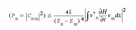
where Pn is the probability of ending in state n
(assuming the initial state is m), Cnm is the matrix
element, E is the energy of a state, H is the system Hamiltonian,
and vn and vm are wave functions. This gives
an upper bound on the probability when the rate of change in the Hamiltonian
( H/t) is a constant over some interval
and zero before and after. Transition probabilities for systems in which H/t increases and decreases smoothly over
a time t >>
H/t) is a constant over some interval
and zero before and after. Transition probabilities for systems in which H/t increases and decreases smoothly over
a time t >>  /E) are much lower; probabilities can also be larger
or smaller after a series of abrupt changes, as phases add or cancel. For the
present analysis, the maximum value of Pn encountered in a
series of sample times, Pn,max, is used to estimate the probability
of occupancy of that state at the end of that time interval. A more detailed
analysis preserving phase information would be of interest, but should for the
present system yield results of the same order as this estimate.
/E) are much lower; probabilities can also be larger
or smaller after a series of abrupt changes, as phases add or cancel. For the
present analysis, the maximum value of Pn encountered in a
series of sample times, Pn,max, is used to estimate the probability
of occupancy of that state at the end of that time interval. A more detailed
analysis preserving phase information would be of interest, but should for the
present system yield results of the same order as this estimate.
The following analysis describes the Hamiltonian and
associated switched-charge wave functions along a
one-dimensional coordinate. Wave functions are computed in the
adiabatic approximation, neglecting the perturbing potential
imposed by acceleration and charge mass (this imposed
potential has a magnitude less than 5 × 10-23 J,
significantly smaller than the potentials imposed by either
the switching charge or the material of the switch). Changes
in this perturbing potential, however, provide a significant
component of
H/t and hence substantially affect
excitation probabilities.
We will call the potential created by the switch gate acting
on the switched charge in the absence of the switching charge
the "underlying potential." This potential is created by
appropriate design of the switch gate. Because the switch
gate is bilaterally symmetric, the underlying potential must
necessarily be bilaterally symmetric as well.
Ideally, the switching charge would steer the switched charge
down the chosen path without changing the shape of the
potential well. From the frame of reference of the switched
electron, almost nothing would have happened and excitation
would be minimal. If the underlying potential were harmonic,
and the potential imposed by the switching charge had a
linear gradient, then the approach of the switching charge
would have exactly this effect (a linear gradient applied to
a harmonic well results in a new harmonic well of the same
width but moved laterally: exactly what we desire).
In practice, the gradient created by a point charge is
nonlinear. To some extent, this can be compensated by
adjusting the underlying potential so that the resulting
total potential (the underlying potential plus the potential
created by the switching electron) is harmonic. This cannot
be done completely, for the underlying potential is
bilaterally symmetric and the wave function of the switched
electron will have a significant component on both sides of
the center of the switch gate (at least during the earlier
phases of switching). However, the region of the underlying
potential in the vicinity of the switched electron and on the
same side of the centerline can be made exactly harmonic by
appropriate modifications to the underlying potential.
Second order terms can be cancelled by appropriate changes in
the underlying potential, but higher-order terms cannot be
cancelled during the early stages of switching, owing to the
symmetry constraint on the underlying potential.
(Effective cancellation of third-order terms becomes feasible
when the switched charge has shifted by more than the
characteristic radius of its ground-state wave function.)
The residual sources of
H/t
include third-order terms (during the early
stages of switching), together with changes in the
acceleration-induced potential and changes in the potential
associated with the growth of a barrier as the incoming well
in the underlying potential splits to form two outgoing
wells.
Structure of the potential
The potential surface analyzed here is not optimized, but is
the product of several cycles of modification aimed at
correcting obvious defects. The potential surface is defined
in terms of two "paths," the path of the switching electron
xswitching(z) and the path of the switched electron
xswitched(z) (where z is a dimensionless quantity). While
the path of the switching electron is exact, the "path" of
the switched electron is only approximate as the wavefunction
of the switched electron is diffuse in the x coordinate. The
function xswitched(z) can therefore be viewed as an arbitrary
function used to define the potential.
The potential combines several distinct components. The first
is the electrostatic potential imposed by the switching
charge:
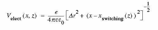
We assume e is 5.7 (corresponding to the dielectric constant
of diamond) and r
is 4 nm (a gap in the
y direction sufficient to reduce cross-channel tunnelling to
low values). The parameter z is a dimensionless
measure of distance along the path, entering into the
dynamical analysis through a choice of
dz/dt.
All other components are part of the underlying potential and
are constrained to be even functions about the midpoint.
These include a harmonic term:

and a recursively-defined correction term:
where
g(z) = -
ksxswitched
(z) and x' =
2xswitched(z) - |x|
This term cancels the difference between the electrostatic
potential and a linear gradient with a slope of
g J/m in the region between x = 0 and x =
2xswitched(z), yielding a total
potential that is exactly harmonic within these bounds.
There does not appear to be a unique "right" choice for the
value of the total potential outside these bounds. We have
(somewhat arbitrarily) chosen the underlying potential so
that
[Vtotal(xswitched(z)+offset, z) -
Vtotal(xswitched(z), z)] +
[Vtotal(xswitched(z)-offset, z) - Vtotal(xswitched(z), z)] =
Vharm(offset) +
Vharm(-offset).
Finally, the walls of the potential well are steepened in
regions where the ground state wave function has a small
amplitude by adding
This term substantially raises the energies of the higher
excited states without greatly affecting the ground state.
These various potentials have more or less randomly altered
the potential at the bottom of the harmonic potential well,
i.e.,
Vtotal(xswitched
(z), z) might vary as z varies. We desire, however, that the
potential at the bottom of the well remain constant. To this
end, we define Vzero(z) as having that
value required to make
Vtotal(xswitched
(z), z) equal 0. Note that Vzero(z) is
a function of z only and does not change as x changes.
The overall potential is:
Vtotal(x,z) =
Vharm(x) +
Velect(x,z) +
Vcorr(x,z) +
Vwall(x,z) +
Vzero(z)
The total potential has continuous first derivatives so long
as the gradient g is numerically equal to
Velect(x,z)/x evaluated at x = 0. This
condition can be maintained during the early evolution of the
potential, but must be violated at later times. The
difference between these gradients defines the magnitude of a
wedge potential (creating a peak at x = 0) that
forms an implicit component of
Vtotal.
Time history of the potential
The evolution of the well potential determines
H/t.
Since the potential is
determined by the positions of the switching and switched
charges, the evolution of the well potential is specified by
choices of xswitching(z)
and xswitched(z). In the
model potential, these functions are the natural cubic
splines (Press et al. 1992) passing through the points
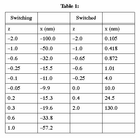
tabulated in Table 1. The resulting paths and potentials are
illustrated in Figures 9 and 10. The speed of switching is
determined by dz/dt (assumed to be
constant). It is often convenient to use the
reciprocal dt/dz, which we call the
characteristic switching time or tchar.
Figures 8, 9 and 10 assume a tchar of 5
ps (i.e., dz/dt of 2 × 10¹¹).
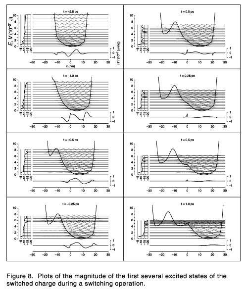
(A larger version of Figure 8 is available).
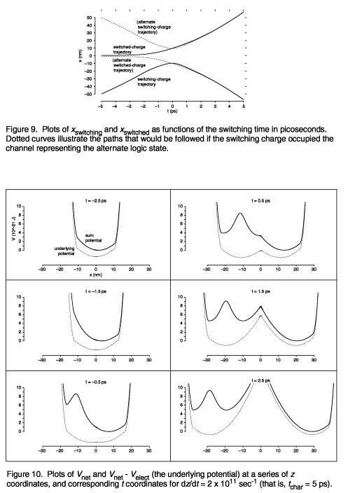
(A larger version of Figure 9 is available).
(A larger version of Figure 10 is available).
Table 1. Defining points of natural cubic splines (Press et
al. 1992) describing the trajectories of switched and
switching charges in the model potential (rounded to three
digit precision). The parameter z is
dimensionless.
In the initial (pre-wedge) phase of the switching interaction
(through z = ~0.05), maintaining a zero wedge
potential makes xswitching and
xswitched functions of one another (a
relationship approximated by the given splines). The
acceleration profile is chosen to limit the the jerk
resulting from the motion of the well minimum. (Note that
the "wedge potential" is not an actual potential, but is
merely a consequence of combining the potentials already
defined. It is useful, however, to give it a name).
In the following (disengagement) phase, the growth of the
wedge potential continues the motion of the switched charge
away from the midplane, and a substantial and growing region
around the well minimum is exactly harmonic. Changes in well
shape outside this region cause residual excitation, but
these decline as the exactly harmonic region expands into the
tails of the ground-state wave function. (In particular, the
discontinuity in the potential gradient associated with the
peak of the wedge results in a fast rate of change of
potential as seen in the well frame.) The disengagement phase
ends as the magnitude of the ground-state wave function at
x = 0 becomes negligible (when z
~ 0.15).
In the final (separation) phase, excitation is small, and
(according to the energy-based error bound described above)
errors are minimized by choosing a design that maximizes the
quantum number n of the lowest excited state
centered in a secondary well. Placement of the switching
charge so as to create two secondary wells of equal depths is
nearly optimal during this phase; in the model potential,
this condition determines xswitching
for z > 0.2. The lowest state that can become bound in
the wrong well, n = 9.
Error rates
Error rates depend on dz/dt.
Estimating error probabilities Perr as
the sum from n = 9 to n = 14 of
Pn,max, for values of
dz/dt corresponding to
tchar = 5, 10, 20, and 40 ps yields values of
~ 9.3 × 10⁻¹¹, 2.3 × 10⁻¹¹, 5.8
× 10 -12, and 1.5 × 10⁻¹²,
respectively. Contributions from states with n
> 14 are small. The near proportionallity of
Perr to
(dz/dt)2 indicates
that jerk contributes little to the excitation, which is
instead dominated by consequences of deviations of
Vnet from exact harmonicity. Even with
tchar = 5 ps,
Perr remains low enough to enable the
construction of digital logic systems of high reliability,
with a modest cost in time and energy dissipation resulting
from error detection and correction.
Energy dissipation due to switching
Energy dissipation occurs when switched charges undergo excitation and deexcitation
(typically with phonon emission). This process is dominated by excitation to n
= 1, which is > 103 times more probable than excitation to any higher
state. The associated energy dissipation Ediss ~ P1,max
× ~ P1,max × 4.6 ×
10-22 J. For tchar = 5, 10, 20, and 40 ps, Ediss
= 1.3 × 10- 26, 2.3 × 10⁻²⁸, 1.7 × 10⁻²⁸,
and 5.2 × 10⁻²⁹ J per switching event. Jerk plays a dominant role
in energy dissipation--but not error rates--at the faster switching speeds, owing
to the greater coupling to low-spatial-frequency features of H/t by n = 1, relative
to n = 9. Each of these values of Ediss is far smaller
than kT at one kelvin (~ 1.4 × 10⁻²³ J). An analysis
retaining phase effects would permit the choice of an acceleration profile resulting
in substantial cancellation of excitation to the n = 1 state, reducing
energy dissipation by ~ 1000 relative to the present estimates.
Input and Output
Another issue is communication with the outside world. If
the active computing element is embedded in a high intensity
rotating electric field then the use of metallic wires poses
obvious difficulties (much as placing a fork in a microwave
oven might be ill advised). It might still be possible to
use wires provided that they are always at right angles to
the electric field. It might be difficult to achieve this,
however, in which case some pickup from the rotating electric
field would still occur. The use of twisted pair would
reduce this problem. Despite the obvious drawbacks, the use
of metallic wires might prove useful.
Another method would be to use fiber optics. This eliminates
concerns about putting wires into an intense rotating
electric field. Simply by having an input fiber which
started well outside the region of the rotating electric
field and terminated within the active region it would be
possible to selectively create electron-hole pairs in the
semiconductor by injecting light into the other end of the
fiber. Absorption of photons can be done in relatively small
structures; for example, a one micron thickness of GaAs can
absorb roughly a third of the incident light(Casey and Panish
1978) page 46]. If the GaAs were part of a helical
structure, the generated electrons and holes would then be
separated by the electric field and would move to opposite
sides of the helix. This method of generating electron-hole
pairs will produce packets of irregular size. By making too
many electrons and holes and then selectively re-combining
unwanted electrons and holes, we could reduce the packet size
to the desired value. Re-combination will occur when the
diameter of the helix becomes small enough to allow the
electrons and holes to recombine. By controlling the
diameter of the helix, the number of electrons and holes that
remain in the packets can be controlled. An alternative
method would be split the helix and allow the packet (through
self repulsion) to break apart into smaller pieces. A
sufficient number of splits would produce packets that had
only a single electron or hole in them. The result would be
several helices each one of which contained exactly zero or
one charge carrier. This rather error-ridden input could
then be converted into a more reliable result using
appropriate logic circuitry.
Having once generated a pair of charge carriers, we could
simply continue to let the pair be switched throughout
further logic operations. Double helical logic would require
the use of two helical paths and two switching elements,
increasing the volume and component complexity. By using
single helical dipole logic (i.e., a single helix carrying
both an electron and a hole to represent a "1") the leading
charge carrier would be switched through a switch gate and
when the electric field rotated through an additional 180
degrees, the second carrier of the pair would be switched in
exactly the same fashion.
For output, we need merely recombine electrons with holes
next to an optical fiber. The optical fiber can then carry
the resulting photons outside the rotating electric field
where conventional detectors and electronics can be used. In
single helix dipole logic, a simple method of combining
electrons and holes would be to terminate a helical path
carrying a pair. The leading charge carrier, upon reaching
the end of the helical path, would be unable to continue.
The trailing carrier would then catch up. When the two met,
the electron and hole would recombine and generate a
photon.
Both input and output, depending on how they're implemented,
might suffer from a relatively high error rate. This can be
corrected by using various coding and multiple transmission
schemes that provide sufficient redundancy to correct the
errors.
Simple, robust I/O using optical methods should be feasible
even in the presence of the strong rotating electric field
required by helical logic.
The optical methods of input and output described here are
highly dissipative. Many entering photons will fail to
generate an appropriate electron-hole pair; when a pair is
generated in the electric field the resulting current flow
will be dissipative; the recombination of electrons with
holes to adjust the size of the charge packet is dissipative;
and when electrons are combined with holes to generate
optical output many of the resulting photons will be lost.
While simple, this method of input and output is far from
reversible and will impose energy limitations on the I/O
bandwidth. It is often feasible in principle for I/O to be
done in a reversible fashion. If two reversible processors
wish to communicate with each other in a logically reversible
manner, then there is no fundamental requirement that the
process be dissipative. Further research is needed to
provide a good low energy method of input and output.
Three main categories of energy dissipation were considered:
transport losses, dielectric losses, and switching losses.
Estimates of fundamental losses per cycle when the external
field has a frequency of 10 gigahertz were made. Transport
losses are primarily acoustic, estimated at below 10-27
joules per cycle.
Dielectric losses vary widely depending on the exact crystal
symmetry, with even the equation describing the loss being
different for different symmetry groups. A rough estimate
for the fundamental dielectric loss for diamond is below
10-35
joules per cycle per switch with an electric field
strength of 108 volts/meter. While pure diamond will almost
certainly have a different (and lower) loss than the highly
structured complex logic circuitry that would be needed in an
actual system, this calculation still suggests that energy
dissipation from this source can be made very small (and can
likely be reduced to below 10-27 joules per cycle, the
dissipation estimated from other loss mechanisms). Further
research on the dielectric loss is required to better
understand and minimize the losses that can be expected from
this mechanism.
Switching losses below 10-27 joules per logic operation at
switching speeds faster than 10-10 s should also be feasible.
These losses involve both the excitation of electrons and
their dissipative return to the ground state, as well as
radiative losses resulting from the accelerations to which
the switched electron is subjected during a switching
operation.
These estimates support the conclusion that thermodynamically
reversible single electron logic operations should eventually
be able to achieve very low energy dissipations, very likely
below 10-27 joules per logic operation at a temperature of 1
K and a speed of 10 gigahertz. The largest energy loss
mechanism identified was acoustic radiation, which could be
reduced by the use of dipoles. Even though the estimates of
dielectric loss and radiative loss were small there is
substantial uncertainty in their values: further analysis
seems appropriate.
Faster Operation
The reader might have noticed that 10-27 J dissipated times
10-10 seconds switching time is 10-37 J-s, significantly
below Planck's constant h = 6.626
× 10-34 J-s. This is not a
violation of any fundamental principles, however(Feynman
1985). If, instead of the energy dissipated we consider the
magnitude of the change in the switching Hamiltonian
H over
the course of a switching operation then we can produce an
energy-time product which does have significance in the
context of the current proposal. The approximate value of
H
is 10-20 J; multiplied by the switching time this gives
10-30 J-s which is larger than Planck's constant by over
three orders of magnitude. This gap suggests that faster
switching should be feasible before any fundamental limits
are encountered.
In the present proposal simply increasing the clock frequency
would result in faster switching times, though at the cost of
increased energy dissipation and error rate since no attempt
was made to keep track of phase information. The switching
time was simply made long compared with the time of a single
oscillation of the first excited state of the switched
electron, thus allowing use of the adiabatic approximation.
If the switching time were ~h/H and if we computed the wave
function of the switched electron as it left the switch, it
should be possible to "catch" the switched electron in an
appropriately designed potential. Switching speeds of ~10-14
s with minimal energy dissipation and error rates should be
feasible using this approach. With lateral movement of the
switched electron of ~10-8 m we have
electron speeds of ~106
m/s (~.003 c), accelerations of ~1020 m/s2,
forces of ~10-11
N, and an electron-electron separation (in vacuum) of ~5 ×
10-9 m. Relativistic effects and materials limitations
should not pose fundamental limitations for operations at
these speeds.
A switching speed faster than ~10-14 s in the context of the
current proposal would require creating a larger switching
potential by, for example, using more than one switching
electron (i.e., a charge packet). Use of a suitable charge
packet would also permit reliable room temperature operation.
More detailed analysis of rapid switching would be of
interest.
Summary
The picture of computing that emerges from this analysis is
relatively simple: a solid block of material that is
intricately designed at the molecular level is placed into a
cavity resonator which has a frequency of several gigahertz.
The resonator and the block of material are kept at low
temperature, perhaps 1 K. Fiber optic connections allow the
block to communicate with the outside world. Photons
generated outside the cavity resonator by conventional
electronics are carried into the block via fiber optics to
create electron hole pairs, which then enter into
computations within the block. By combining electrons with
holes, photons can be generated within the block which are
then carried out of the cavity resonator by fiber optics and
detected by conventional electronics. The cavity resonator
has a high Q, and the computations within the block of
material produce relatively little additional energy loss. A
significant source of energy loss in this particular proposal
is in the I/O, which is quite dissipative. If the number of
I/O operations is relatively small compared with the number
of total logic operations performed or if some method of I/O
can be found which dissipates much less energy (which seems
likely) then the total energy dissipation per logic operation
can be made remarkably small.
Conclusions
Projections of current trends in energy dissipation per gate
operation(Landauer 1988) suggest that the kT "barrier" will
become significant within a few decades. This barrier can be
overcome by using reversible logic. Further, the trend
towards decreasing device size and increasing device
precision will likely result in atomically precise logic
elements which employ single electrons, single holes, or both
to carry the 0's and 1's of a computation. Helical logic is
the first proposed member of the class of single electron
thermodynamically reversible atomically precise logic
devices. Members of this class might mark the ultimate
evolution of electronic devices. Helical logic also avoids
many of the problems of conventional clock distribution.
The energetic costs of charging and discharging clock lines
might otherwise become a significant source of energy
dissipation in future computing devices. A preliminary
analysis suggests that the energy dissipation of helical
logic can be reduced below 10-27 joules per logic operation
at a switching speed of 10 gigahertz and an operating
temperature of 1 K. Further reductions in energy dissipation
might be feasible if double helical logic is used. The
estimates of dielectric loss and radiative loss were both
well below 10-27 J, but had significant uncertainties that
require further examination. Further research to develop the
highly precise manufacturing technologies needed to
economically fabricate this (and other) proposed computing
technologies is needed(Merkle 1994). Further investigation
of single electron, thermodynamically reversible, atomically
precise logic devices seems warranted.
Acknowledgements
The authors would like to thank J. Storrs Hall, Rolf
Landauer, Alan Lewis, Norman Margolus, Jim Mikkelsen, John
Northrup, Ed Richley, Jeff Soreff, Robert Thornton, Tommaso
Toffoli, and Chris van de Walle.
References
-
Bean, J. C. (1992) Proceedings of the IEEE, Vol. 80 No. 4,
April. Silicon-Based Semiconductor Heterostructures: Column
IV Bandgap Engineering
-
Bennett, C. H. (1973) IBM Journal of Research and
Development, 17, 525-532, November. Logical Reversibility of
Computation
-
Bennett, C. H. (1982) International Journal of Theoretical
Physics, Vol. 21, No. 12 905-940. The Thermodynamics of
Computation - A Review
-
Bennett, C. H. and Landauer, R. (1985) Scientific American,
July, 48-56. The Fundamental Physical Limits of
Computation
-
Bennett, C. H. (1988) IBM J. Research and Development, Vol.
32, No. 1, January, 16-23. Notes on the History of Reversible
Computation
-
Bennett, C.H. (1989) SIAM J. Computing, Vol. 18, No. 4, 766-
776, August. Time/Space Trade-offs for Reversible
Computation
-
Bobeck, A. H. and Scovil, H.E.D. (1971) Scientific
American, June, Vol. 224, No. 6, 78-91. Magnetic Bubbles
-
Bohm, D. (1951) Quantum Theory (Prentice Hall).
-
Braginsky, V. B., Mitrofanov, V. P. and Panov, V. I. (1985)
Systems with Small Dissipation (University of Chicago
Press).
-
Braginsky, V. B., Ilchenko, V. S., and Bagdassarov, Kh. S.
(1987) Physics Letters A, Volume 160, No. 6, March 2, 300-
305. Experimental observation of fundamental microwave
absorption in high-quality dielectric crystals
-
Carter, F.L, Siatkowski, R.E. and Wohltjen, H. eds., (1988)
Proceedings of the 3rd International Symposium on
Molecular Electronic Devices (North-Holland).
-
Casey H. C. and Panish, M. B. (1978) Heterostructure Lasers
(Academic Press).
-
Drexler, K. E. (1988) in Proceedings of the 3rd International
Symposium on Molecular Electronic Devices, F.L. Carter, R.E.
Siatkowski, H. Wohltjen, eds. (North-Holland). Rod Logic and
Thermal Noise in the Mechanical Nanocomputer
-
Drexler, K.E. (1992) Nanosystems: Molecular Machinery,
Manufacturing, and Computation (Wiley Interscience).
-
Feynman, R.P. (1960) Caltech's Engineering and Science,
February. Also see
http://www.zyvex.com/nanotech/feynman.html. There's Plenty
of Room at the Bottom
-
Feynman, R. P., Leighton, R. and Sands, M. (1963) (Addison
Wesley). The Feynman Lectures on Physics, Vol. I
-
Feynman, R. P. (1985) Optics News, February, 11-20. Quantum
Mechanical Computers
-
Fredkin, E. and Toffoli, T. (1978) November 1978 DARPA
proposal. Design Principles for Achieving High-Performance
Submicron Digital Technologies
-
Fredkin E. and Toffoli, T. (1982) International Journal of
Theoretical Physics, Vol. 21, Nos. 3/4, 219-253. Conservative
Logic
-
Grabert H. and Devoret M. H. (eds) (1992) Single Charge
Tunneling (Plenum Press)
-
Gurevich, V. L. (1979) Sov. Phys. Solid State 21(11),
November, 1993-1998. Dielectric Losses in Crystals
-
Gurevich, V. L. and Tagantsev, A. K. (1991) Advances in
Physics, Vol. 40, No. 6, 719-767. Intrinsic dielectric loss
in crystals
-
Hall, J.S. (1992) Laboratory for Computer Science Research,
Rutgers University, Proceedings of the Workshop on Physics
and Computation, October 2-4, 237-247 (IEEE Press).
Electroid Switching Model for Reversible Computer
Architectures
-
Halliday, D. and Resnick, R. (1988) The Fundamentals of
Physics, Extended Third Edition (Wiley).
-
Israelachvili, J. (1992) Intermolecular and surface
forces, second ed. (Academic Press)
-
Kinoshita, K., Sasao, T. and Matsuda, J. (1976) IEEE
Transactions on Computers, Vol. C-25, No. 3, March, 247-253.
On Magnetic Bubble Logic Circuits
-
Koller, J. G. and Athas, W. C. (1992) Proceedings of the
Workshop on Physics and Computation, October 2-4, 267-270
(IEEE Press). Adiabatic Switching, Low Energy Computing, and
the Physics of Storing and Erasing Information
-
Landauer, R. (1961) IBM Journal of Research and Development,
Vol. 6, July 1961, 183-191. Irreversibility and Heat
Generation in the Computing Process
-
Landauer, R. (1981) in Sixth International Conference on
Noise in Physical Systems, Mejier, P.H.E., Mountain, R. D.,
Soulen Jr., F. J. eds [Nat. Bur. Stand. (U.S.), Publ. 614]
12. Fundamental Physical Limitations of the Computational
Process
-
Landauer, R. (1988) Nature, Vol. 335, October 27, 779.
Dissipation and noise immunity in computation and
communication
-
Likharev, K. K. (1982) International Journal of Theoretical
Physics, Vol. 21, Nos 3/4, 311 to 326. Classical and Quantum
Limitations on Energy Consumption in Computation
-
Likharev, K. K. and Claeson, T (1992) Scientific American
Vol 266 No. 6, June, 80-85. Single Electronics
-
Likharev, K. K., Rylov, S. V. and Semenov, M. K. (1985) IEEE
Transactions on Magnetics, Vol. MAG-21, No. 2, March, 947-
950. Reversible Conveyer Computation in Array of Parametric
Quantrons
-
Merkle, R. C. (1992) Proceedings of the Workshop on Physics
and Computation, October 2-4, 227-228 (IEEE Press). Towards
Practical Reversible Logic
-
Merkle, R. C. (1993a) Nanotechnology 4, 86-90. A Proof
about Molecular Bearings
-
Merkle, R.C. (1993b) Nanotechnology 4 114-131. Two Types Of
Mechanical Reversible Logic
-
Merkle, R. C. (1993c) Nanotechnology 4, 21-40. Reversible
Electronic Logic Using Switches
-
Merkle, R. C. (1994) in: The Ultimate Limits of Fabrication
and Measurement, Welland, M. E. and Gimzewski, J. K. eds.
(Kluwer, Dordrecht). Self Replicating Systems and Low Cost
Manufacturing
-
Press W. H., Teukolsky S. A., Vetterling W. T., and Flannery
B.P. (1992) (Cambridge University Press). Numerical
Recipes in FORTRAN: the art of scientific computing,
second ed.
-
Ressler, A.L. (1981) Master's Thesis, Department of
Electrical Engineering and Computer Science, Massachusetts
Institute of Technology, January. The Design of a
Conservative Logic Computer and a Graphical Editor
Simulator
-
Sakaki, H. (1980) Japanese Journal of Applied Physics, Vol.
19 No. 12, December, L735-L738. Scattering Suppression and
High-Mobility Effect of Size-Quantized Electrons in Ultrafine
Semiconductor Wire Structures
-
Seitz, C. L., Frey, A. H., Mattisson, S., Rabin, S. D.,
Speck, D. A., van de Sneepscheut, Jan L. A. (1985) Chapel
Hill Conference on VLSI, Computer Science Press, 1-17. Hot-
Clock nMOS
-
Soreff, J. (1994) private communication.
-
Sze, S. M.(1990) High-Speed Semiconductor Devices (Wiley
Interscience).
-
Van de Walle, C. G. (1989) Physical Review B, volume 39,
Number 3, January 15, II, 1871-1883. Band lineups and
deformation potentials in the model-solid theory
-
Washburn, S. (1992) Nature Vol 357, May 21, 199-200. Single
atoms as transistors
-
Younis, S. G. and Knight, T. (1993) AI Laboratory, MIT,
preprint. Practical Implementation of Charge Recovering
Asymptotically Zero Power CMOS
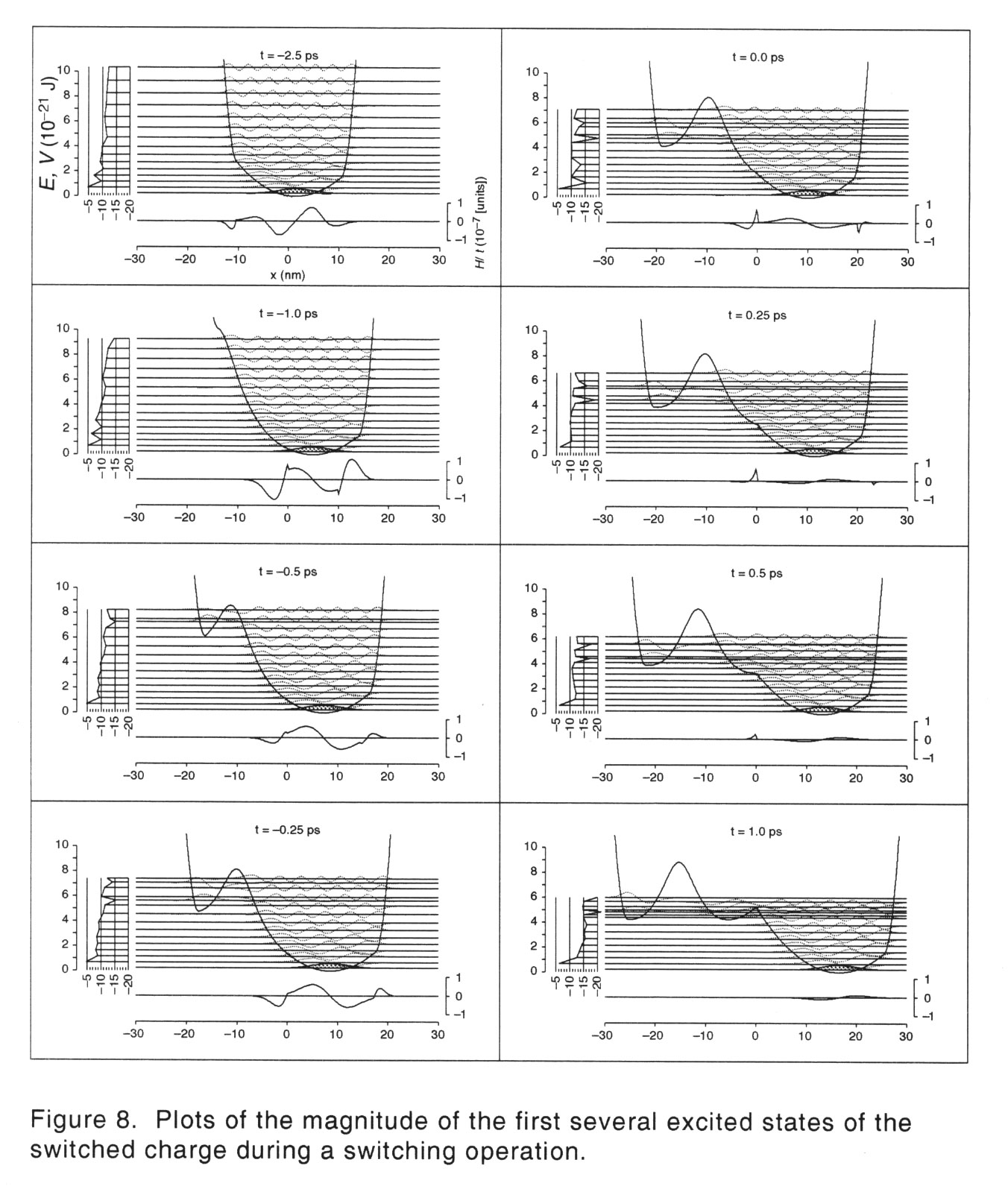
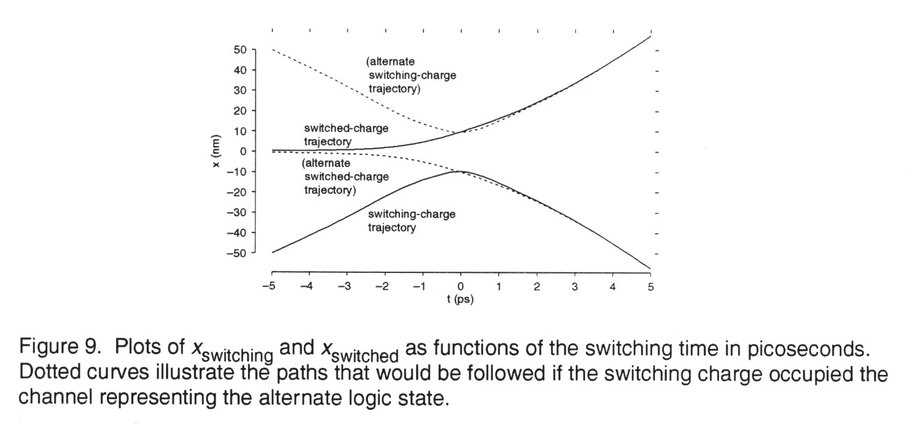